ASTM E1476
Standard Guide for Quantitative Analysis by Energy-Dispersive Spectroscopy Read More


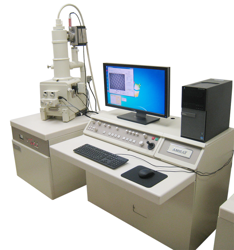
Unlock the secrets of your materials with our state-of-the-art Scanning Electron Microscope (SEM). Designed for precision and versatility, this advanced SEM utilizes a focused beam of high-energy electrons to deliver stunningly high-resolution images of surface topography and composition. Perfect for metallurgy, it excels in analyzing the microstructure and composition of metals and alloys, making it an essential tool for material characterization.
Featuring a uniquely large chamber, our SEM accommodates various sample sizes and configurations, allowing for both high and low vacuum environments. This adaptability ensures optimal imaging conditions for every specimen. Additionally, the built-in Energy Dispersive Spectroscopy (EDS) detector measures X-rays, enabling you to identify and quantify the elements present in your samples with unparalleled accuracy.
Elevate your research and analysis capabilities with our Scanning Electron Microscope, where high performance meets innovative design, allowing you to uncover the intricacies of your materials like never before.
Standard Guide for Quantitative Analysis by Energy-Dispersive Spectroscopy Read More